HUB75-style RGB panels have no framebuffer of their own. The controller must continuously shift color bits, latch them, select a row address, and control output enable. An FPGA is a strong match because those deadlines can be expressed as a deterministic state machine. This tutorial explains the interface and builds the safe row-scan sequence.
The signal groups
VHDL-2008 reference implementation
This article uses synthesizable VHDL-2008. The complete tested VHDL bundle is linked below; adapt clock constraints, I/O standards, and timing parameters to the target board and panel.
library ieee;
use ieee.std_logic_1164.all;
use ieee.numeric_std.all;

entity hub75_row_scanner is
  generic (COLUMNS : positive := 64; ROW_GROUPS : positive := 16);
  port (
    clk       : in  std_logic;
    rst       : in  std_logic;
    dwell_done: in  std_logic;
    pixel_bits: in  std_logic_vector(5 downto 0);
    hub_clk   : out std_logic;
    lat       : out std_logic;
    oe_n      : out std_logic;
    row_addr  : out natural range 0 to ROW_GROUPS - 1;
    rgb       : out std_logic_vector(5 downto 0)
  );
end entity;

architecture rtl of hub75_row_scanner is
  type state_t is (blank, shift_low, shift_high, latch, set_row, display);
  signal state : state_t := blank;
  signal col   : natural range 0 to COLUMNS - 1 := 0;
  signal row   : natural range 0 to ROW_GROUPS - 1 := 0;
begin
  process (clk)
  begin
    if rising_edge(clk) then
      if rst = '1' then
        state <= blank; col <= 0; row <= 0;
      else
        case state is
          when blank      => col <= 0; state <= shift_low;
          when shift_low  => state <= shift_high;
          when shift_high => if col = COLUMNS - 1 then state <= latch; else col <= col + 1; state <= shift_low; end if;
          when latch      => state <= set_row;
          when set_row    => state <= display;
          when display    => if dwell_done = '1' then if row = ROW_GROUPS - 1 then row <= 0; else row <= row + 1; end if; state <= blank; end if;
        end case;
      end if;
    end if;
  end process;

  hub_clk  <= '1' when state = shift_high else '0';
  lat      <= '1' when state = latch else '0';
  oe_n     <= '0' when state = display else '1';
  row_addr <= row;
  rgb      <= pixel_bits when state = shift_low else (others => '0');
end architecture;
Download the VHDL-2008 FPGA LED controller examples
- R0/G0/B0 and R1/G1/B1: two RGB pixels shifted in parallel, usually for an upper and lower row.
- CLK: shifts one column of color data.
- LAT or STB: transfers the shift register into the output latch.
- OE: output enable, commonly active-low.
- A–E: binary row address; the count depends on the panel scan ratio.
Panel naming is not a complete electrical specification. Verify the connector, logic voltage, scan ratio, channel order, and timing on the exact unit. Some panels swap green and blue or use a nonstandard address arrangement.
One safe row transaction
- Drive OE inactive to blank the outputs.
- Shift one bit per color channel for every column.
- Pulse LAT while outputs remain blanked.
- Set the row address and allow it to settle.
- Drive OE active for the desired dwell time.
- Blank again before the next latch or row transition.
Blanking around latch and address changes is the main defense against ghosting. The interval can be short, but it must be explicit and repeatable.
A row-scan state machine
Production logic should register memory output ahead of the shift edge and constrain the external clock and data relationship. The conceptual FSM above makes signal ownership and blanking easy to review.
First-light test pattern
Start with one row and solid primary colors. Then display vertical stripes that change every column, followed by a single moving pixel. These patterns reveal channel swaps, column direction, row-address errors, and off-by-one clock counts much faster than a photograph.
Power and logic levels
A panel can draw several amperes at 5 V. Power it through its intended connector with appropriate wiring and ground return; do not route LED current through an FPGA board header. Many controller boards use level shifting between 3.3 V FPGA I/O and 5 V panel logic. Confirm the exact panel requirements before connection.
Panel references
Timing diagram: blank before changing state
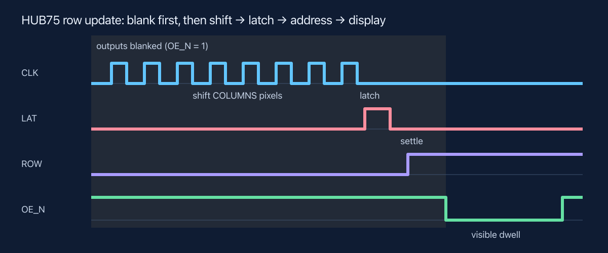
A controller that follows this ownership sequence makes ghosting much easier to reason about. The output latch never changes while LEDs are visible, and the address bus receives a defined settling interval before output enable becomes active.
Self-check the transaction
The reference testbench asserts that LAT never pulses while outputs are enabled, counts exactly one shift-clock rising edge per column before each latch, and observes the row address wrapping after the configured number of groups.
Calculate the refresh budget before adding color
The row transaction is repeated for every bitplane and every row group. Use the interactive HUB75 timing calculator to see how panel width, scan ratio, pixel clock, overhead, and BCM depth change the maximum full-frame refresh rate.
FPGA LED controller tutorial series
This article is part of the FPGA LED Controller Tutorials learning path. Continue with PWM vs. BCM, the HUB75 timing calculator, or VHDL-2008 verification.
Leave a Reply