An LED scanner reads pixels continuously while a CPU, DMA engine, or animation core writes the next image. If both sides touch the displayed image, the panel can show half of one frame and half of another. A double buffer fixes tearing: one memory bank is scanned while the other is updated, and ownership changes only at a frame boundary.
The architecture
Front bank: read by the real-time display scanner.
Back bank: written by the producer.
Swap request: says the back bank contains a complete frame.
Frame boundary: the only place the scanner changes banks.
The producer must not write the bank currently being scanned. The scanner must not switch until the last row and last bitplane have completed.
Infer two synchronous memories
localparam int PIXELS = WIDTH * HEIGHT;

logic [23:0] bank0 [0:PIXELS-1];
logic [23:0] bank1 [0:PIXELS-1];
logic        front_bank;
logic [23:0] scan_pixel;

always_ff @(posedge write_clk) begin
    if (write_en) begin
        if (front_bank) bank0[write_addr] <= write_data;
        else            bank1[write_addr] <= write_data;
    end
end

always_ff @(posedge scan_clk) begin
    if (front_bank) scan_pixel <= bank1[scan_addr];
    else            scan_pixel <= bank0[scan_addr];
end
This example writes the bank opposite front_bank. If the clocks are unrelated, do not pass front_bank directly into write logic without a synchronization and ownership protocol. A safer system acknowledges each swap back to the producer before accepting more writes.
Swap only on a complete frame
always_ff @(posedge scan_clk) begin
    if (rst) begin
        front_bank <= 1'b0;
        swap_ack   <= 1'b0;
    end else if (frame_done && swap_pending) begin
        front_bank <= ~front_bank;
        swap_ack   <= ~swap_ack;
    end
end
A toggle acknowledgement is easier to cross between clock domains than a one-cycle pulse. The producer holds the back bank stable after requesting a swap and waits until it sees the acknowledgement toggle.
Account for memory latency
Block RAM normally has a synchronous read. Request pixel N one clock before its bits are needed, and pipeline the column counter, plane index, and row metadata alongside the data. An off-by-one memory pipeline often appears as a one-column horizontal shift.
Capacity example
A 64×32 RGB framebuffer at 24 bits per pixel contains 49,152 bits. Double buffering requires 98,304 bits before padding and parity. Compare that requirement with the block-RAM geometry of the target FPGA, not only its headline memory total.
Constant-current LED drivers move current regulation and grayscale timing closer to the LEDs. The FPGA sends brightness words, controls shift and latch signals, and supplies any required grayscale clock. This tutorial uses TI’s TLC5940 and TLC5955 as concrete examples while keeping the controller architecture reusable.
Know what the driver provides
Device
Channels
Grayscale
Serial rate
TLC5940
16
12 bit
Up to 30 MHz
TLC5955
48
16 bit
Up to 25 MHz
The TLC5940 uses an external grayscale clock and exposes BLANK, XLAT, error, and programming-mode behavior. The TLC5955 adds 16-bit grayscale, per-color brightness controls, dot correction, error detection, and display-repeat features. The exact bit packing and edge timing come from the selected datasheet—not from a generic SPI assumption.
A reusable shift-and-latch engine
typedef enum logic [2:0] {IDLE, LOAD, CLK_HI, CLK_LO, LATCH, DONE} state_t;

always_ff @(posedge clk) begin
    case (state)
        IDLE: if (start) begin
            shift_reg <= frame_data;
            bit_count <= FRAME_BITS-1;
            state <= LOAD;
        end
        LOAD: begin
            sin   <= shift_reg[bit_count];
            sclk  <= 1'b0;
            state <= CLK_HI;
        end
        CLK_HI: begin
            sclk  <= 1'b1;
            state <= CLK_LO;
        end
        CLK_LO: begin
            sclk <= 1'b0;
            if (bit_count == 0) state <= LATCH;
            else begin bit_count <= bit_count - 1'b1; state <= LOAD; end
        end
        LATCH: begin
            lat   <= 1'b1;
            state <= DONE;
        end
        DONE: begin
            lat   <= 1'b0;
            done  <= 1'b1;
            state <= IDLE;
        end
    endcase
end
Parameterize frame width and bit order, then wrap the engine with a device-specific formatter. Register all outputs and constrain the interface as real external timing paths.
Initialization sequence matters
Hold outputs blank while clocks and configuration stabilize.
Program current range, brightness control, and dot correction before grayscale data.
Load a known all-zero frame and latch it.
Start the grayscale clock or display-repeat function.
Release blanking only after a complete valid frame is active.
Electrical and thermal checks
The current-setting resistor, LED supply, output compliance voltage, simultaneous-channel current, package power dissipation, and PCB copper determine safe operation. Do not choose LED current from RTL. Calculate it from the device equations and verify worst-case thermal conditions.
An LED scanner often runs from a deterministic display clock while pixels arrive from a CPU bus, DMA engine, USB bridge, or network clock. Passing a “new frame” pulse or a multibit control word directly between those domains can cause lost events, metastability, and torn frames. This tutorial builds a safe frame-swap handshake.
Synchronizers solve only single-bit sampling
A two-register chain in the destination domain reduces the probability that metastability escapes into user logic. It does not make a changing multibit bus coherent, and a narrow source pulse can disappear entirely between destination clock edges.
(* ASYNC_REG = "TRUE" *) logic req_meta, req_sync;

always_ff @(posedge scan_clk) begin
    req_meta <= swap_request_toggle;
    req_sync <= req_meta;
end
Use a toggle for an event
The producer flips a bit after finishing the back buffer. The scanner synchronizes that bit and compares it with the last value it serviced. The event persists until observed, regardless of the relative clock rates.
logic serviced_toggle;
logic swap_pending;

always_ff @(posedge scan_clk) begin
    if (rst) begin
        serviced_toggle <= 1'b0;
        swap_pending     <= 1'b0;
    end else begin
        if (req_sync != serviced_toggle)
            swap_pending <= 1'b1;

        if (frame_done && swap_pending) begin
            front_bank      <= ~front_bank;
            serviced_toggle <= req_sync;
            swap_pending    <= 1'b0;
            ack_toggle      <= ~ack_toggle;
        end
    end
end
Synchronize ack_toggle back into the producer domain. The producer must not overwrite the completed back buffer until it observes the acknowledgement.
Move multibit data safely
Use a dual-clock FIFO for a stream of pixels or commands.
Use dual-port memory plus ownership handshakes for framebuffers.
For a stable configuration bus, hold the bus unchanged from request through acknowledgement and capture it only after the synchronized request.
Never synchronize each bit of a bus independently; different bits can settle on different cycles.
Constraints and structural checks
Mark recognized synchronizer registers with the vendor-supported attribute, declare asynchronous clock relationships correctly, and run the tool’s CDC report. A false-path constraint hides timing analysis; it does not create safe hardware. Review every reported crossing and confirm the RTL structure matches the protocol.
Verification strategy
Run source and destination clocks at non-integer ratios.
Randomize request timing around destination edges.
Assert every accepted request receives exactly one acknowledgement.
LED display bugs are unusually visual: a single missed clock becomes a shifted column, an unsafe latch becomes a flash, and a clock-domain error becomes a torn frame. The fastest path to a fix is to translate the visible symptom into a timing hypothesis, then prove or reject it with a test pattern, assertion, oscilloscope, or logic analyzer.
Symptom-to-cause map
Symptom
Likely causes
Whole display flickers
Low refresh rate, irregular frame timing, power droop
Faint previous row
OE active during latch or address change, insufficient blanking
Image shifted one column
Wrong clock count, block-RAM latency, data changed on wrong edge
Red and blue exchanged
Connector or bit-order mismatch
Horizontal tear
Framebuffer changed before frame boundary
Low-level shimmer
LSB dwell too short, jitter, unsynchronized brightness update
Camera bands
Refresh interaction with exposure or rolling shutter
Use diagnostic patterns
Solid red, green, and blue reveal channel mapping.
Alternating columns reveal shift direction and off-by-one clocks.
A single moving pixel reveals row/column addressing.
One bitplane at a time reveals dwell-weight errors.
A gray ramp reveals gamma, missing low bits, and framebuffer format mistakes.
Probe the timing contract
Capture CLK, LAT, OE, row address, and at least one color data line. Trigger on LAT. Count column clocks between latches, measure how long OE remains active for each plane, and confirm the row address is stable before light is enabled. A passthrough adapter or spare test points make this much easier than probing a ribbon cable.
Turn expectations into assertions
// Outputs must be blank while latching.
assert property (@(posedge clk) lat |-> oe_n);

// A bank swap is legal only at the frame boundary.
assert property (@(posedge clk) $changed(front_bank) |-> $past(frame_done));

// The serializer emits exactly COLUMNS rising edges per row/plane.
assert property (@(posedge clk) latch_event |-> shift_count == COLUMNS);
Separate logic faults from electrical faults
If the FPGA waveform is correct but the panel is not, inspect voltage levels, ground bounce, cable length, edge rate, current-supply wiring, and connector orientation. Reduce brightness and display one channel; if the failure changes with total current, power integrity is a stronger suspect than bitplane math.
A disciplined debug order
Verify the clock and reset.
Verify active polarities with a static output.
Count shifts and check data setup around the external clock.
Check blank-latch-address-enable ordering.
Measure row and frame rates.
Enable one bitplane, then add planes.
Add framebuffer swaps only after static frames are clean.
Finally test maximum brightness, cable length, and camera behavior.
Change one variable at a time and save known-good captures. LED controllers become manageable when every visible artifact is tied back to a small timing contract that can be measured.
An FPGA can drive an LED display in two very different ways: send every PWM bitplane on a strict schedule, or send complete intensity values to a driver that generates PWM internally. The pixels may look identical, but the timing, bandwidth, and failure modes are not.
External PWM makes the controller responsible for both pixel data and the timing of the light output.
The difference in one sentence
External PWM sends a timeline; internal grayscale sends a value. In the first architecture, the controller decides exactly when each bitplane is visible. In the second, the controller writes an intensity word and the driver turns that value into pulses.
Question
External PWM bitframes
16-bit grayscale driver
What crosses the interface?
One bit per channel, once per bitplane
One complete intensity word per channel
Who schedules PWM?
FPGA or microcontroller
LED driver
Traffic for a static image
Continuous
Usually only the initial load
Timing freedom
High
Defined by the driver
Main design risk
Missed real-time deadlines
Update and latch behavior
External PWM bitframes
With external PWM, the FPGA or microcontroller decomposes every channel value into bitplanes. For an N-bit value, plane 0 contains every channel’s least-significant bit, plane 1 contains the next bit, and so on. Each plane is displayed for a time proportional to its binary weight: 1, 2, 4, 8 … up to 2N-1.
This technique is also called binary coded modulation, bit-angle modulation, or bitplane PWM. The display driver can be simple—it shifts, latches, and enables outputs—but the controller must continuously meet the shift-clock, latch, row-select, blanking, and output-enable deadlines.
Small Verilog example: select one bitplane
// 8-bit RGB value for one pixel; plane runs from 0 to 7.
wire [7:0] red   = pixel_rgb[23:16];
wire [7:0] green = pixel_rgb[15:8];
wire [7:0] blue  = pixel_rgb[7:0];

assign serial_rgb = { red[plane], green[plane], blue[plane] };
The extraction is easy. The harder logic is the scheduler around it: load a plane, blank the outputs, latch it, select the row, enable it for the weighted interval, and repeat without jitter.
Driver-managed 16-bit grayscale
A grayscale-capable driver accepts a complete intensity word for each channel and stores it internally. A local timing engine compares those stored values against a grayscale counter and produces the output pulses. The controller updates the image; the driver keeps refreshing it.
A grayscale driver accepts intensity words and generates the high-rate PWM locally.
This turns a continuous waveform-generation job into a frame-update job. Once a frame is loaded, the driver can display it while the FPGA calculates the next image, services another interface, or simply waits.
Small C example: write one 16-bit channel
static void write_grayscale(uint16_t level)
{
    spi_write((uint8_t)(level >> 8));
    spi_write((uint8_t)(level));
}

write_grayscale(0x6000);  // about 37.5% of full scale
A real driver may pack channels differently and may require a latch or frame-boundary signal, so its datasheet still controls the exact transaction.
Bandwidth: count payload bits first
For C color channels, B bitplanes, and a PWM refresh rate of F, the minimum external-bitplane payload is:
external payload = C × B × F bits/s
A 64 × 32 RGB panel has 6,144 channels. At 12-bit color and 200 complete PWM cycles per second, the raw payload is about 14.7 Mbit/s before latch, blanking, addressing, or protocol overhead. That traffic continues even when the picture is static.
For a 16-bit grayscale driver updated at U frames per second:
grayscale update payload = C × 16 × U bits/s
The same panel updated at 60 frames per second needs about 5.9 Mbit/s of raw intensity data. Hold the image still and the update traffic can fall to zero while the driver continues its PWM. Update all 16 bits at 200 frames per second, however, and the raw payload rises to about 19.7 Mbit/s. Internal PWM is not automatically lower bandwidth; its advantage is that display refresh is decoupled from image updates.
Timing pressure grows faster than bit depth
The bitplane count grows linearly with resolution, but the weighted time range grows exponentially. A 12-bit PWM cycle contains 4,095 least-significant-bit time units; a 16-bit cycle contains 65,535. Ignoring scan multiplexing and overhead, the shortest slot is:
TLSB = 1 ÷ [F × (2B − 1)]
At 200 Hz and 12 bits, that is about 1.22 µs before row scanning, blanking, latching, and settling time take their share. This is why the least-significant planes are often where a design first shows brightness errors, flicker, or lost effective bits.
What each architecture buys you
External PWM
Full timing control: choose plane order, blanking, refresh strategy, and effective depth.
Room to experiment: temporal dithering, camera synchronization, and custom compensation live in FPGA logic.
Simple output devices: shift-register-style drivers can be inexpensive and transparent.
The cost: continuous traffic, more memory and scheduling logic, and hard real-time deadlines.
Internal grayscale PWM
Lower controller workload: send intensity data and let dedicated hardware perform modulation.
Stable local timing: PWM is isolated from unrelated controller stalls and arbitration.
Efficient static display: stored values can be reused indefinitely.
The cost: less control, a more capable driver, and device-specific latch and buffering rules.
Which should you choose?
Choose external PWM when modulation itself is part of the design: you need deterministic custom timing, unusual plane ordering, camera-aware refresh, or the freedom to trade color depth against refresh dynamically. It is a natural fit when the FPGA already has enough I/O bandwidth, RAM, and timing margin.
Choose a grayscale driver when you want a clean frame-oriented boundary, stable high-resolution brightness, and less continuous work in the controller. Verify whether the device double-buffers its grayscale memory, when new data takes effect, whether outputs must be blanked during latching, and how its PWM clock relates to your required refresh rate.
The deciding question is not simply “How many bits?” It is where should the timing contract live? External bitframes keep it in programmable logic. A grayscale driver moves it next to the LEDs.
I’ve recently been learning more and more about FPGA development and VHDL. It’s quite different from what many software engineers think “programming” is. FPGA’s require a different mindset for everything. There are no data structures, there are no bytes, there isn’t even any numbers. The only thing you have is bits. You have physical metal pins on the FPGA that handle inputs and outputs and they can send or receive physical bits (0 or 1).
The way you write the design is also different. Internally, everything is basically just flip-flops. We also have this new found concept of a “clock” which is alien to programmers who don’t ever touch hardware.
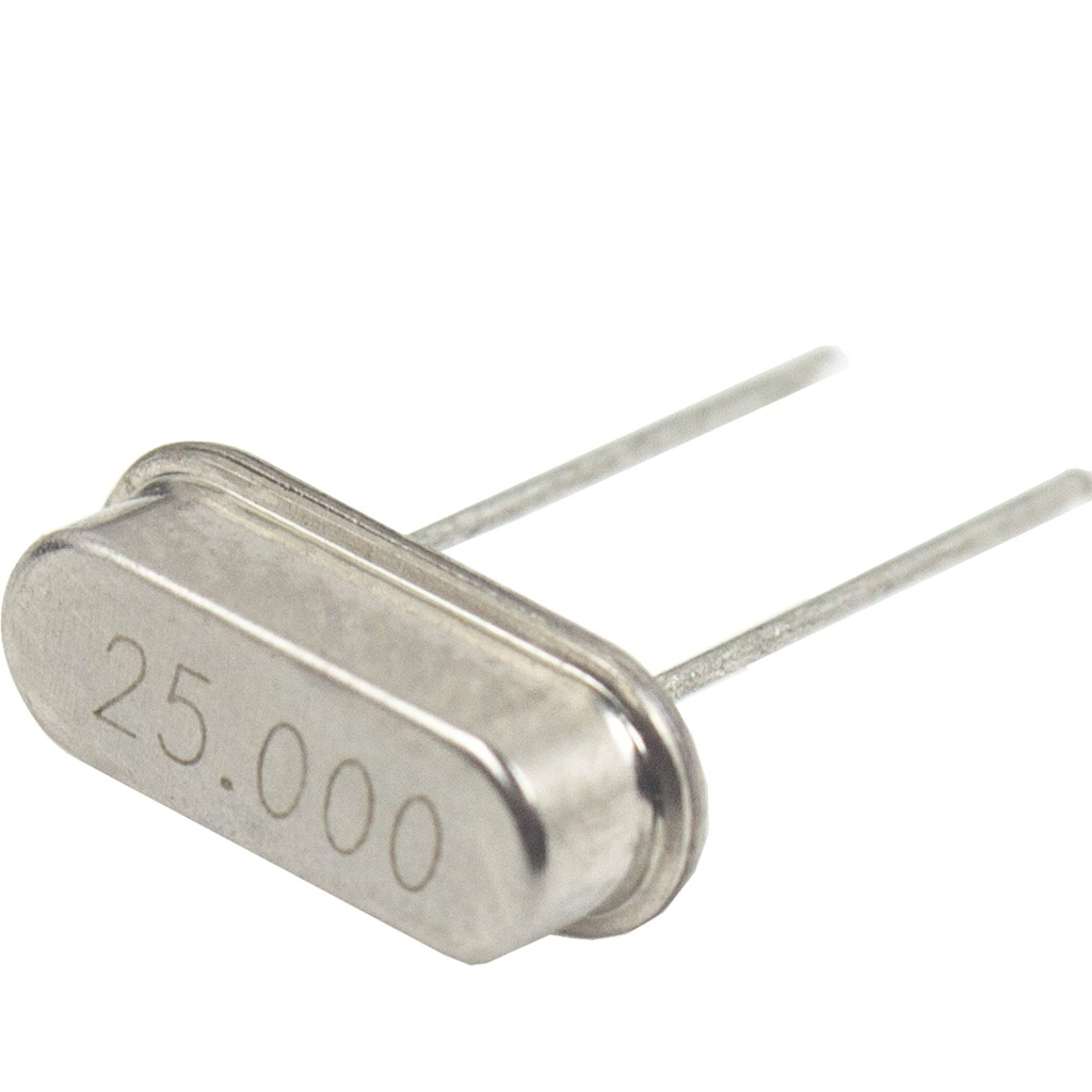
What is a clock? A clock is generally something like a crystal osc which is on the board. Heres an image of a 25 Mhz crystal osc.
This thing has a piece of quartz crystal inside of it which vibrates at 25 million times per second, thus, 25 Mhz. There are varying speeds for the crystal oscillators, from 25, 50, 125, and even higher. They also have varying prices for the cost of these physical components. The 25 Mhz clock is quite useful because it can be used to do 1G ethernet.
A PLL is a phased lock loop. It’s basically a way to use a clock to make more clocks. You can create “synthetic” clocks from a real clock. The way it works is simple. Let’s say you have a 25 Mhz clock. 1G ethernet needs a 125 Mhz clock. So, you can create a PLL clock with the source being the 25 Mhz clock and multiply it by 5 which will give you a 125 Mhz clock.
Anyways, I might expand more upon this at a later point, but, this is quite interesting stuff.
Used to monitor number of Google Analytics server requests
10 minutes
__utmb
Used to distinguish new sessions and visits. This cookie is set when the GA.js javascript library is loaded and there is no existing __utmb cookie. The cookie is updated every time data is sent to the Google Analytics server.
30 minutes after last activity
__utmc
Used only with old Urchin versions of Google Analytics and not with GA.js. Was used to distinguish between new sessions and visits at the end of a session.
End of session (browser)
__utmz
Contains information about the traffic source or campaign that directed user to the website. The cookie is set when the GA.js javascript is loaded and updated when data is sent to the Google Anaytics server
6 months after last activity
__utmv
Contains custom information set by the web developer via the _setCustomVar method in Google Analytics. This cookie is updated every time new data is sent to the Google Analytics server.
2 years after last activity
__utmx
Used to determine whether a user is included in an A / B or Multivariate test.
18 months
_ga
ID used to identify users
2 years
_gali
Used by Google Analytics to determine which links on a page are being clicked
30 seconds
_ga_
ID used to identify users
2 years
_gid
ID used to identify users for 24 hours after last activity
24 hours
_gat
Used to monitor number of Google Analytics server requests when using Google Tag Manager
1 minute
_gac_
Contains information related to marketing campaigns of the user. These are shared with Google AdWords / Google Ads when the Google Ads and Google Analytics accounts are linked together.
90 days
__utma
ID used to identify users and sessions
2 years after last activity
You can find more information in our Cookie Policy and .